
Hot Press News
- PRMS Billing Solutions Expands Nationwide Medical Billing & RCM Services to 25+ Specialties
- Mahindra's Largest Dealer in India, PPS Motors Inaugurates a new showroom at Camp, Pune
- Factech Introduces New AI Agent to Automate CAFM workflows
- Awtomated TBMS launched Intelligent Workflow and AI Automation for LSPs
- Union Minister of Textiles Inaugurates Bharat Tex 2026
- Fintec Markets Launches Multi-Broker Support, Giving Traders the Freedom to Choose Their Preferred Broker
- Medilink Healthcare Services Expands Comprehensive Home Healthcare Support for Families Across Behala and Joka
- Mahabir Danwar Jewellers announce “Couple No 1” Season 5 with a Grand Prize Trip to Baku
- BC.Game Clone Script Trends Up as BC.GAME Launches Star Wins with 1,024 Winning Ways
- Indonet Group Highlights INDODRAIN Geonets for High-Capacity Drainage in Infrastructure Projects
- A 79-country study measures where crypto is used out of need, not enthusiasm
- iCallify Launches Scalable IP PBX Software for Modern Business Communication
- Softaken Debuts Free Online Tool to Convert Photos to Grayscale Instantly
- The Purple Turtles, Beruru and Oorjaa Announce the Annual Sale 2026
- ARM MLM Launches AI-Powered Binary MLM Software to Transform Network Marketing Automation
 Mail to a Friend Mail to a Friend |
|
 |
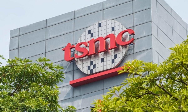
TSMC Once Again Broke Through the Limits of Semiconductor Materials
2026-07-14 03:10:14
Technology
2100
TSMC once again broke through the limits of Semiconductor Materials, one step further from 1nm.
As silicon-based semiconductors are approaching their physical limits, the industry is looking for other alternative materials. Recently, research conducted by National Taiwan University in collaboration with TSMC and the Massachusetts Institute of Technology found that two-dimensional materials combined with semi-metallic bismuth can achieve extremely low contact resistance, close to the quantum limit, and published this research finding in the journal Nature. This is a huge breakthrough for semiconductor manufacturing processes below 1nm.
The current mainstream semiconductor process has developed to 3nm and 5nm, and even IBM has recently launched 2nm. The number of transistors per unit area is now approaching the physical limit of silicon. Although the breakthrough of the manufacturing process is restricted by the production equipment, there are also factors related to semiconductor materials.
Two-dimensional materials such as graphene have been regarded as materials for next-generation semiconductors since their discovery, but most two-dimensional materials have been unable to replace silicon-based semiconductors due to the limitations of high resistance and low current. The MIT team first discovered that the combination of two-dimensional materials and semi-metal bismuth can effectively reduce resistance and improve current transmission efficiency.
TSMC?s technology research department then optimized the bismuth deposition process. Finally, the NTU team used a helium ion beam lithography system costing tens of millions of dollars to successfully reduce the component channel to the nanometer level before reaching this research result.
It is worth mentioning that the two-dimensional material used in this paper is molybdenum disulfide (MoS2), and its contact resistance has reached 123-ohm microns by combining with semi-metal bismuth.
This multinational cooperation started in 2019 and lasted for one and a half years. The National Taiwan University research team participating in this transnational research is the National Taiwan University Institute of Optoelectronics. Professor Wu Zhiyi from the Organic Optoelectronic Materials Analysis and Research Laboratory and others participated in the research.
The main projects of the laboratory are materials such as graphene, solar cells and OLED. Wu Zhiyi mentioned that after using bismuth as the key structure of the metal electrode, the transistor performance of the two-dimensional material can be comparable to that of silicon-based semiconductors, and it can be compatible with the current mainstream silicon-based process technology, which helps to achieve a breakthrough in Moore's Law. Although it is still in the research stage, the power-saving and high-speed features it provides have great potential.
The leading researcher of MIT is Dr. Pinjun Shen, who is also the first author and corresponding author of this paper. He said that after switching to two-dimensional materials, the process can be broken to below 1nm, which is closer to the limit of the thickness of solid-state semiconductor materials. The material properties of semi-metallic bismuth can eliminate the barriers on the surface of the two-dimensional material, thereby achieving ultra-low contact resistance, and the deposition of semi-metallic bismuth does not destroy the atomic structure of the two-dimensional material.
From this breakthrough, we can see how much TSMC has invested in industry-university research-its industry-university alliance program has united many famous universities to study semiconductor technology. For example, in March this year, TSMC and Taiwan Jiaotong University jointly developed the thinnest boron nitride two-dimensional insulating material, which can also be used for breakthroughs in the 1nm process.
User :- Rachel Ye
Email :-fadjdagd@gmail.com
Url :- https://www.apogeeweb.net/industry-news/tsmc-broke-limits-of-semiconductor-materials.html

Get your Explainer Video at 100 dollars only Today.


To ensure stability and reachability of your applications at all times, remote DDoS protection can keep your hosting services online